


Preface
To reach the goal of net-zero emissions by 2050, nations around the world are expressing their aim to ban gas cars in 2035 (2040 for most countries) one after another, which opens up the demands for new energy cars. Driven by the trend of popularization of electric vehicles, currently the applications of automotive semiconductors not only cover integrated circuit (IC), optoelectronic components (LED/VCSEL/PD), and sensors, but also go deeper to the core power system. Power devices and modules play a critical role in inverters, on board charger (OBC) and power factor correction. In addition, wide band-gap (WBG) components, like SiC (Silicon Carbide) and GaN (Gallium Nitride), significantly increase “switching efficiency” and “power density.” That being said, the lifetime and reliability will be challenged under the operation of “high frequency loss” and “high voltage, high current.”
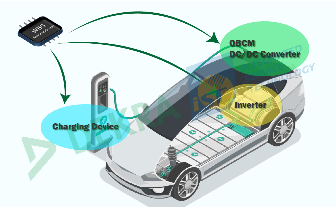
Figure 1: applications of WBG components in an EV drive system
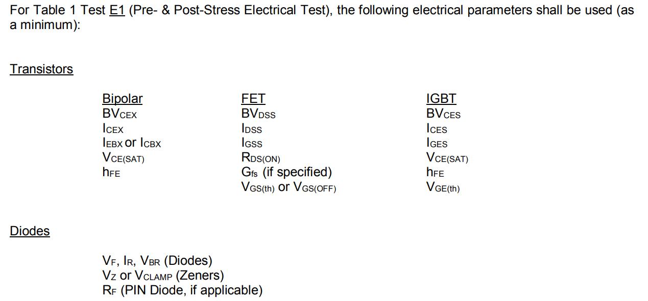
I. Evaluation of the characteristics of power devices is key to determine the specification of product applications.
Straightforward from the application aspects, the power devices allow the semiconductors to switch between conduction (on) and interdiction (off) states. Besides, losses caused by fast switching, capability of dissipating switching load in a circuit, and capacity and mechanism in short-circuit protection are essential parameters as evaluation items.
1. Conduction and interdiction (static parameters)
These parameters consist of“on-resistance” value (Ron), drain cut-off current (IDSS), and breakdown voltage (BVDSS). The characteristics and gain of gate (IGSS & Vth) are also important reference for users’ applications and design.
Source: AEC-Q101
Figure 2: Key parameters for power devices
2. Switching Losses (dynamic parameters)
Double pulse testing enables a sample power switch to be turned on and
off at conducting and blocking states. The keys to evaluate losses include turn-on times, turn-on delays, or even reverse recovery time.
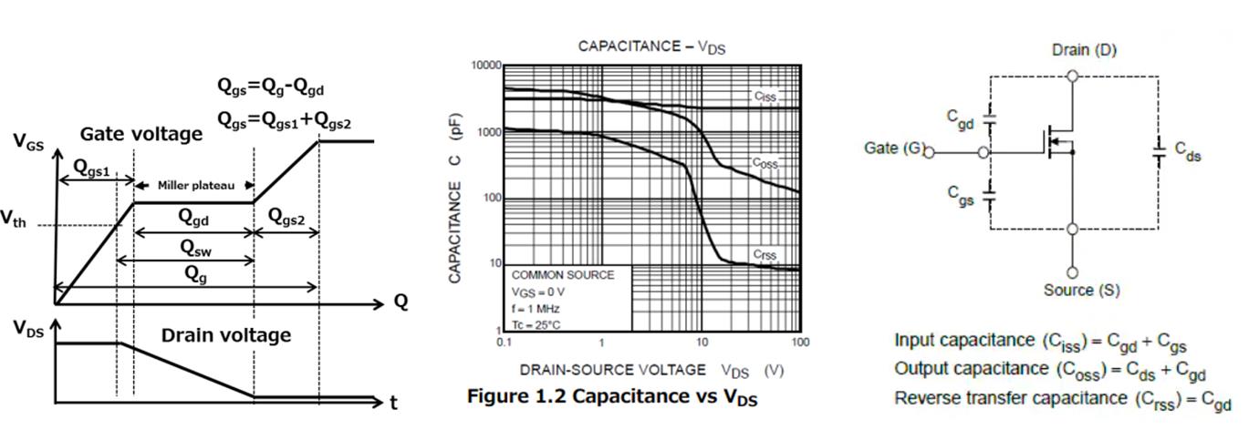
3. Parasitic Inductance/ Capacitance and Gate Charge
At high frequencies, parasitic effects are amplified. One can delve into the sources of losses if having the capacity in the measurement of the following parameters.
Parasitic capacitance (eg. Cgd, Cgs) in an open-circuit path: It is closely linked to the charging energy required for turning on the gate.Double pulse testing enables a sample power switch to be turned on and
off at conducting and blocking states. The keys to evaluate losses include turn-on times, turn-on delays, or even reverse recovery time.
3. Parasitic Inductance/ Capacitance and Gate Charge
At high frequencies, parasitic effects are amplified. One can delve into the sources of losses if having the capacity in the measurement of the following parameters.
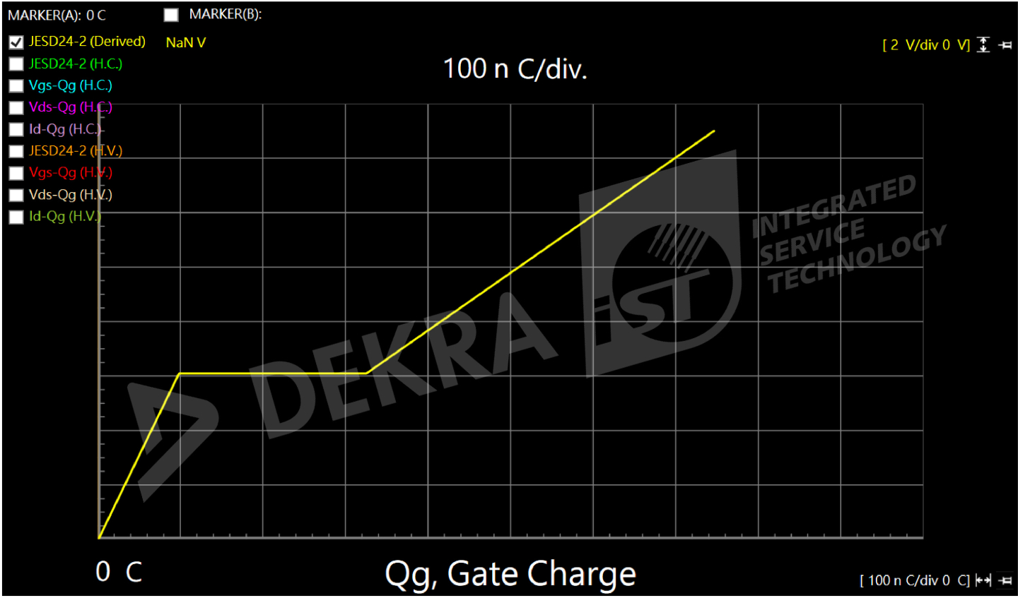
Figure 3: Qg measurement
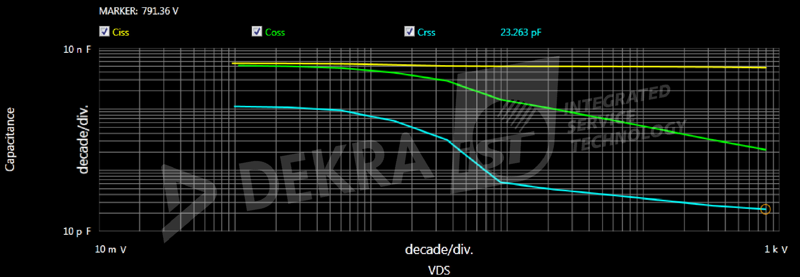
Figure 4: Parasitic capacitance measurement
Source: Toshiba
Parasitic inductance (eg. Lp) in a closed-circuit path: An electromotive force created by inductance in a circuit will result in voltage spikes and delays in blocking time.
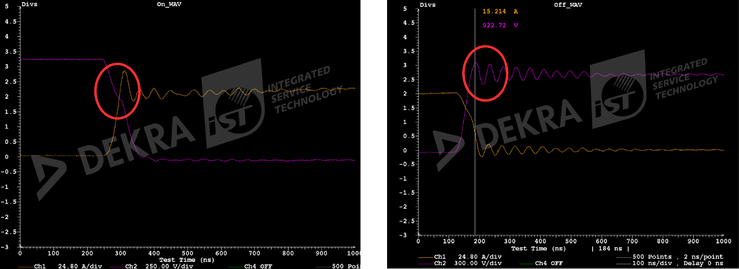
Figure 5: Lparasitic measurement
4. Unclamped Inductive Switching (UIS) and Short Circuit (SC)The following conditions should be considered to ensure that the energy level under real operations meets the requirements for end applications.
Unclamped Inductive Switching: For device applications in a non half-bridge circuit, the inductor is first charged, and then the device is turned off, causing the inductor to dissipate all of its stored energy. High voltage and high current may happen simultaneously in a short period, which can be used to test the endurance level of the sample.
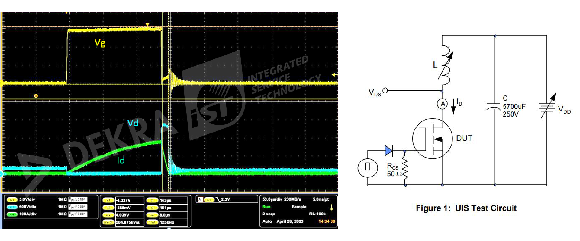
Source: AEC-Q101-004-Sec.2
Figure 6: Evaluation of unclamped inductive switching
Short Circuit: It can occur in a power system, either due to external system abnormalities or device misactivation. Prior to the activation of a protection system (OCP, OverCurrent Protection), the device may experience a momentary surge of high current. With the evolution of material characteristics, the reduction of chip sizes, as well as decreased on-state resistance, the short circuit withstand strength of wide band-gap products is relatively lower compared to traditional Si-IGBTs. Proper evaluation is inevitably a necessary process to prevent system damages.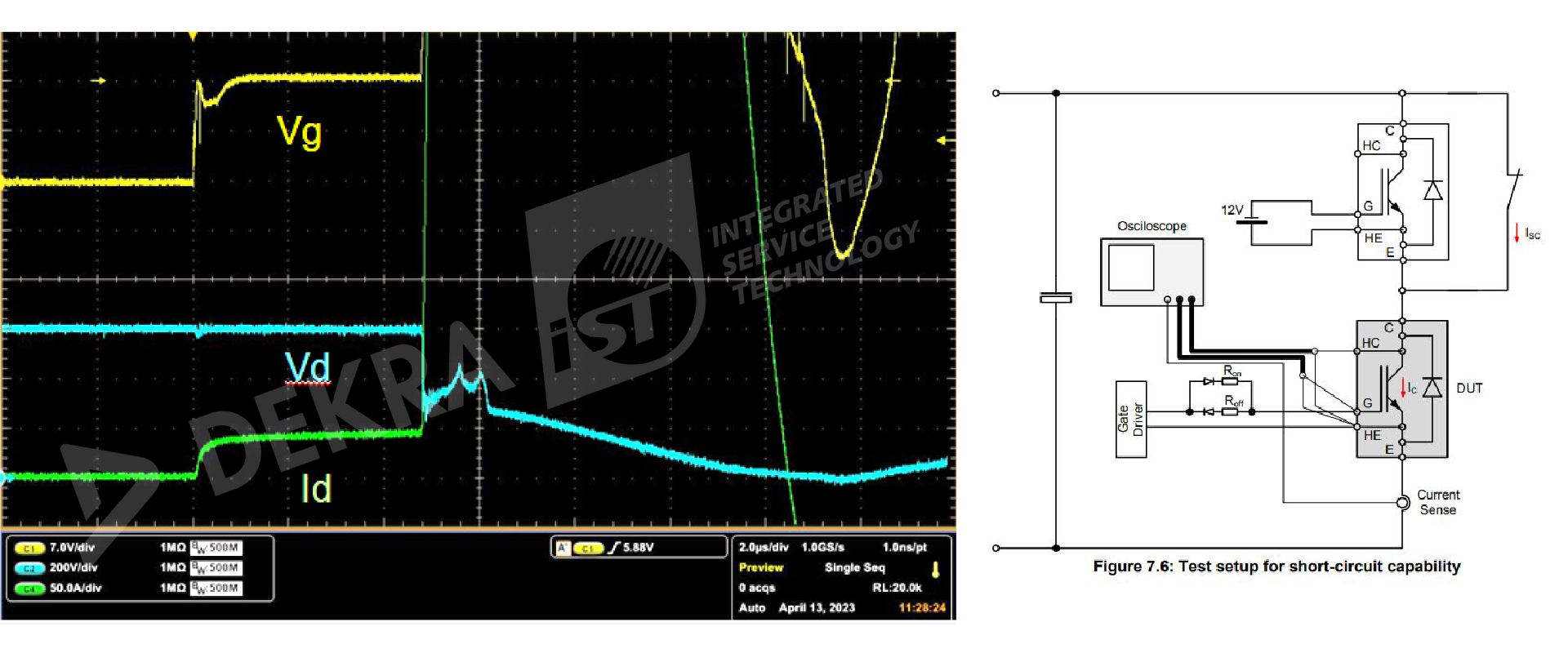
Source: AQG324
Figure 7: Short circuit evaluation
II. Reliability testing conditions of power devices should be upgraded to fit real application environments.
- High Temperature Reverse Bias (HTRB): It is one of the most critical test items for reliability. Device samples are biased with drain-source reverse voltage at an ambient temperature close to their maximum TjMAX. Performance degradation or breakdowns under such bias stress over a long time will be monitored and the device’s working life cycle in applications will also be speculated.
- High Temperature Gate Bias (HTGB): HTGB test simulates potential stress conditions in real applications when gate bias voltage is applied on the device at high temperature. The purpose of this test method is to evaluate the performance and reliability of a device under high temperature and gate bias stress, examining issues that may lead to performance degradation or breakdowns.
- High Humidity High Temperature Reverse Bias (H³TRB): This test is conducted to evaluate the operation capability of a packaged device under high temperature and high humidity. Device samples are stressed at drain-source voltage to verify the resistance to humidity and corrosion of the packaging materials and internal wires for electronic components or modules without encapsulation. Besides, the failure modes of internal corrosion, oxidation, and short circuits will also be identified.
- Thermal Cycling (TC): Devices are put to test in which the temperature is regularly altered, touching a high-temperature peak and a low-temperature peak. The contributing factor that affects reliability is coefficient of thermal expansion (CTE). There is a larger difference between CTE of chips (3ppm/℃) and CTE of boards/ PCB (10~14ppm/℃). Upon repeated cycles of high/low temperature (meaning multiple thermal expansions), the difference of how chips and boards react to temperature makes the materials tensile and leads to fatigue failure, ultimately causing solder joint failure.
- Intermittent Operating Life (IOL): A device goes through on/off cyclic DC power pulse which heats the device junction to a predefined temperature, and subsequently to an off-state junction temperature (Tj). Unlike the thermal cycling test (TC), heating is not done through the ambient temperature but by regulating power level to increase or decrease junction temperature. This test, noticeably, is found more similar to actual situations. In other words, different materials have different CTE under operation. They will not be deliberately heated up just to make all of them reach the CTE at the same temperature. As the failure points are different, and they may eventually result in cracks or breakups of the die-attach layer, this is the main reason that it is mandatory to submit power devices to IOL.
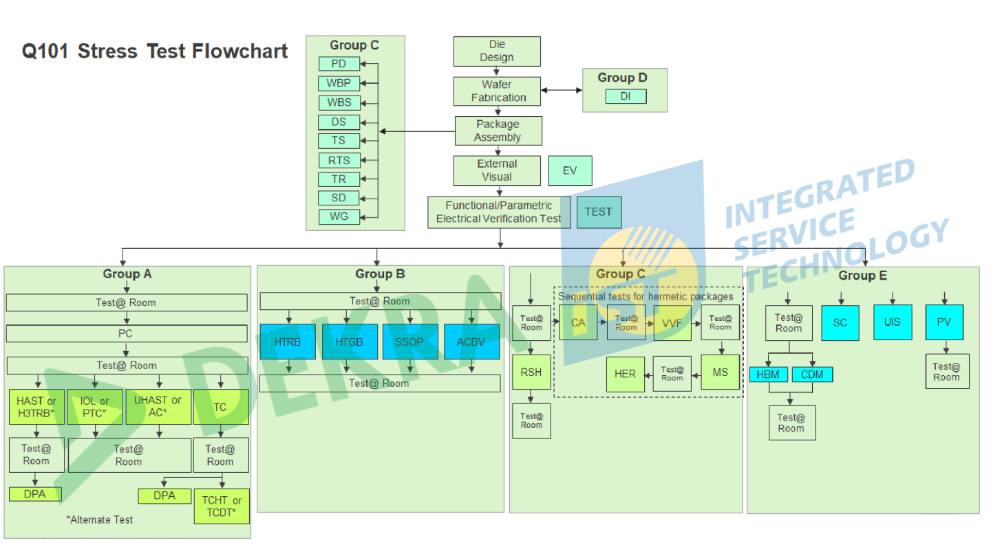
Source: AEC-Q101
Figure 8: EC-Q101 Stress Test Flowchart
Other important items that also work to the actual operation modes and AQG 324 standards are,
- Power cycling and intermittent operating life (IOL):
Temperature rise/decline cycling in junction temperature (T-j) is triggered by on/off states. Stress tests will take place in different areas of a packaging structure at different cycling times. For example, power cycling for quick start-up time (PCsec, Ton<5sec) can be used to evaluate the ruggedness on the wire end; power cycling for long start-up time (PCmin, Ton>15sec) can be employed to asses die attach and bonding quality.
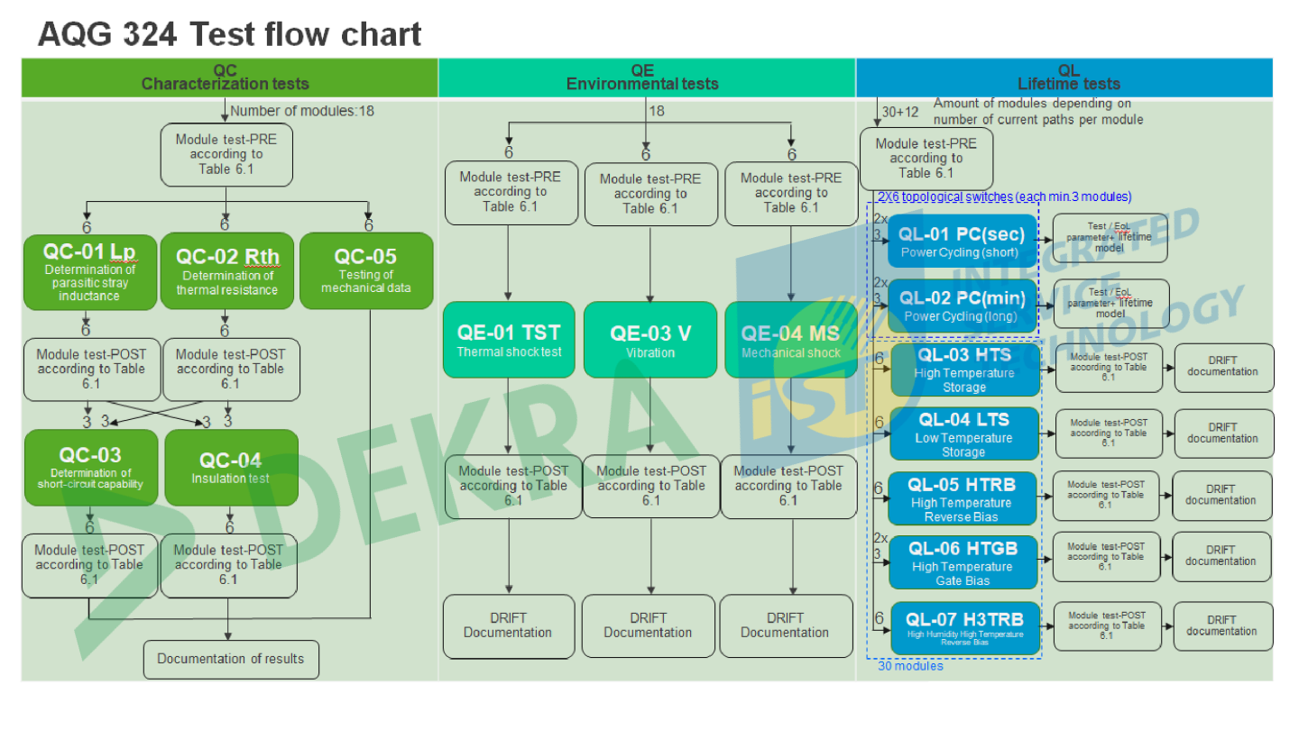
Source: AQG324
Figure 8: Quickly understand the testing workflow and sample number
Another new testing item is the switching reliability test that is used to test GaN devices.
- Dynamic high temperature operating life (DHTOL): The UIS test may induce avalanche effect, so it is not recommended for GaN FETs. Therefore, JEP180.01 defines the dynamic high temperature operating Life (DHTOL) test as a mandatory test for GaN power devices. It explores the reliability of the devices under switching conditions in applications. The real DHTOL test supports accurate models that precisely incorporate test boards and device characteristics with parasitic elements, providing an advanced environment to assess GaN switching behavior and stability. In order to evaluate and validate the current and voltage peaks that define switching stress conditions, the JEP180.01 standard includes: (1) stress testing for switch reliability, (2) switching trajectories and their usage, (3) lifetime modeling and estimation for switching stress.
III. A right partner helps enhance speed to market and wins more business opportunities.
At present, Europe, the U.S., and China are aggressively developing wide band-gap semiconductors. On top of reducing carbon emissions, power device suppliers should also be focused on automotive reliability level of high safety. Most standards deliver the minimum reliability guidelines, whereas DEKRA iST especially suggests inspecting product specifications from long-term perspectives. Reliability validation helps identify failure modes from which defects in processes, materials, or packaging can be improved, in order to pursue high quality at zero defect.
DEKRA iST sees “Bring Quality to Trust” as mission. Customers are well served with comprehensive and professional validation services that are dedicated to solve their pain points. DEKRA iST is committed to offering comprehensive validation solutions to wide band-gap semiconductors in one stop, from parameter analysis, dynamic measurement, high voltage monitoring, and thermal management and analysis on the R&D side to reliability validation requirements of AEC-Q101 (devices), AQG324(modules), and JED180.01 at the validation phase.
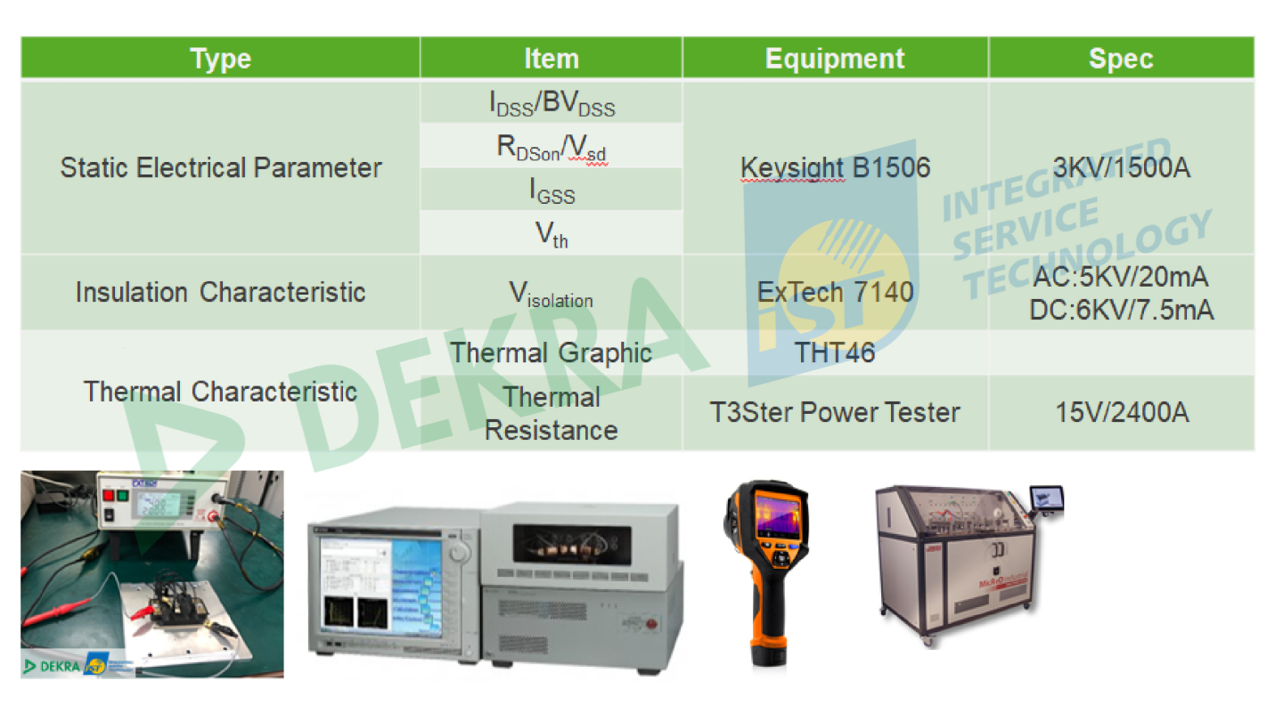
Figure 9: Overview of DEKRA iST’s capacity

To make all your PROBLEMS SOLVED, we provide professional consultant and service.
For more information or service, please feel free to email to 📧 sos@dekra-ist.com


