

PCB has been developed for decades. In 2006 the implement of Lead Free Process in the assembly of electronic products make the assembly temperature of both Reflow and Wave Soldering to increase, as well as the increase of thermal stress. The potential impact of traditional PCB is more serious, and the root cause to make system product failure (Defect) is getting worse than Pb process before; although many material suppliers have developed High Tg based material and improved filter material to overcome the thermal stress problem, many unpredictable issue occur, such as reduced Bond Pad Strength, poor drilling quality, and Conductive Anode Filament (CAF) increase, etc. Therefore, the reliability validation of PCB is important and must be considered seriously.
In addition to the problems arising after the introduction of the lead-free process, various international organizations are also actively promoting halogen-free products in response to environmental protection. Under the dual requirements, PCB manufacturers must meet the lead-free process specifications and also have to satisfy the halogen-free requirements. In view of this situation, DEKRA iST, as a partner with clients, develops a turnkey solution of reliability verification for PCB product (include material characteristics), and provide clients not only validation during design phase, but also monitor production quality by sampling.
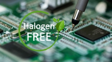
Total Solution for Halogen-fee PCB
- Temperature Cycling Test and Dynamic Low-Resistance Measurement
<IPC-TM-650 2.6.6 conditions>
- Liquid/Air Thermal Shock Test
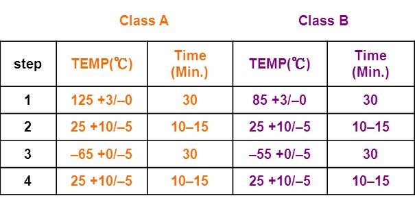
The difference between TST and traditional TCT is that temperature alteration is gradual in TCT, which aims to manifest structural problems of the product by way of CTE mismatching. In TST, the transit time between different temperatures is only 10 seconds, and this short interval is insufficient for manifesting CTE mismatch. The purpose of TST is inducing material failure of the sample as a result of rapid temperature changes.
There are two types of TST chamber: liquid chamber and air chamber; and both types comprise double chambers (cold zone and hot zone). As a sample is moving from one chamber to another, the reside time includes the transit time and sample arrival must achieve the required temperature within two minutes. According to test conditions suggested in IPC-TM-650 method 2.6.7, FR4 materials use condition D and FR5 materials use condition E; total number of cycles depends on IPC specified suggestions with a minimum of 100 cycles.
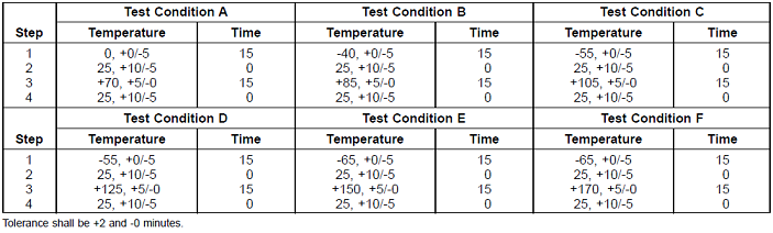
<IPC-TM-650 2.6.7 conditions>
- Electrochemical Migration Test
ECM is a phenomenon when a metal migrates to another polarity via ionization, with dendrite deposits formed causing short-circuits, or that ionized metal compound extends within inner layers of the PCB, reaching another conductor to form a connection. The difference between the two conditions is the reaction equation; the location of the migration can be on surface of PCB or within PCB layers. For testing surface migrations, the test is Surface Insulation Resistance (SIR); for testing migrations between the surface and an internal layer, or between the internal layers, the test is Conductive Anode Filament (CAF).
Comb design PCB or real product both can be executed SIR/CAF tests, and using the comb design PCB is helpful in using less samples and providing more complete observation of the product, which are more helpful in qualifying new suppliers.
The CAF results of Halogen-free PCB is poorer than traditional FR4 or High Tg FR4 materials, and the main reason is material properties and an adverse influence to the quality of PCB drill or laminate process which further raises CAF risks.
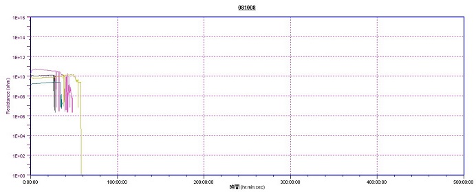
<Real-time monitoring resistance changes>
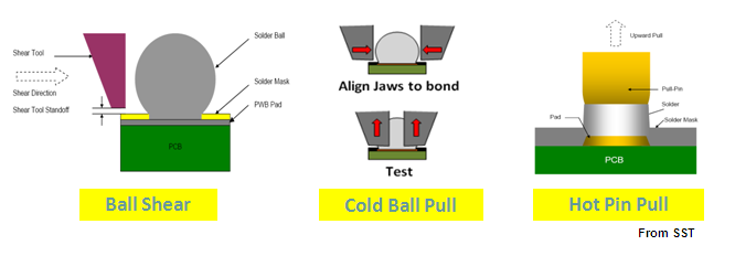
- Copper Trace Tension Test and solder pad bond strength test
Using the Solder Pad Bonding Strength Test is more significance mainly because the test condition is similar to the real product, being capable of simulating the risk of peeling off of solder pads during the maintenance process after the assembly.
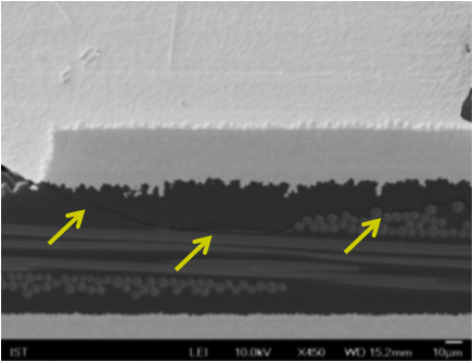
<Pad cratering phenomenon of Halogen-free PCB>
So IPC-9708 has been created, but no acceptance specification is set for this test item; the standard deviation of test data or Cpk is normally used to measure its quality stability. Historical data can also be used for results comparison.
For halogen-free materials, most documentations use the Peeling Test to make observations, bounding strength of these materials is deemed weaker than that of typical FR4 materials. However test results observed from solder pad strength test are not positively related with that of peeling tests.
<IPC-9708 three methods for pad cratering>
- Simulation of Heat Resistance

<IPC-TM-650 2.6.27 reflow set-up condition>
- CTE and Tg Measurement
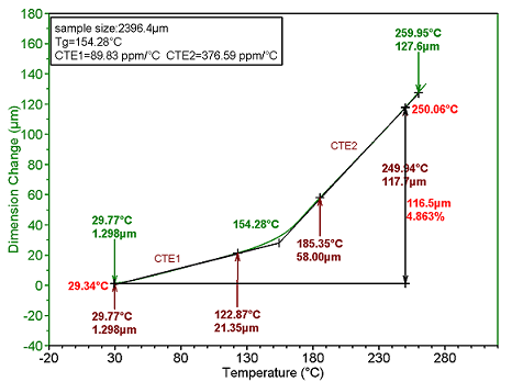
<Coefficient of Thermal Expansion example>
- Bending Test
For portable products, the most frequently used bending tests are cyclic bending, for the purpose of simulating material fatigue when the product is subject to a continuous bending. In addition, the PCB can be tested with components assembled, for observing solder joints affected by the strain resulting from the external force exerting on the PCB during the test. Typical problems like pad peeling and pad cratering can be revealed through this test.
In addition, with single bend and continuously stress by different displacement, Halogen-free board appears the higher hardness than FR-4, and via daisy chain monitoring, the number of defects found in Halogen-free boards is clearly higher than that in traditional high Tg FR4 boards under the same bending stress.
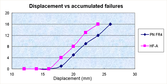
<Comparation of PN FR4 & HF-A testing>
- Mechanical Shock Test
- Faiure Analysis
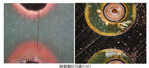
<CAF, Conductive Anode Filament, phenomenon>
DEKRA iST currently executes PCB reliability test in accordance with IPC-TM-650, including chemical tests, mechanical tests, environmental/reliability tests and SMT assembly simulations. DEKRA iST not only provides comprehensive validation to clients, but also offers the expertise consultant of relevant technology and failure analysis.
To make all your PROBLEMS SOLVED, we provide professional consultant and service.
For more information or service, please feel free to email to 📧 sos@dekra-ist.com


