

DEKRA iST adopts advanced technology for PCB failure analysis, such as Focus Ion Beam (FIB) and Cross-section Polisher (CP) for observing micro structures in order to prevent minor phenomenon from being blurred by the ductile copper material during PCB cross-section process. Auger Electron Spectroscopy (Auger) and X-ray photoelectron spectroscopy (XPS) are used for detecting little material on surface and support customer to find root cause of defect as possible. Scanning Electron Microscopy (SEM) and Energy Dispersive Spectrometer (EDS) are effective tools to decrease production/assembly risks and clarify early failure issues, as an example to verify Black Pad phenomenon. In addition, there are other equipment, including Thermal Mechanical Analyzer (TMA), Atomic Force Microscope (AFM), etc, and very helpful to PCB failure analyses as well.
DEKRA iST not only provides failure analysis with high-tech equipment, but also offers the expertise consultant. With comprehensive experiences from each field and diverse product, DEKRA iST helps customers to clarify the problems and suggest possible solutions for PCB improvement. The below is an example for brief Failure Analysis Flow.
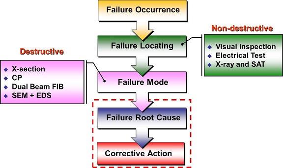
<Failure Analysis Flow>
To make all your PROBLEMS SOLVED, we provide professional consultant and service.
For more information or service, please feel free to email to 📧 sos@dekra-ist.com


