

Major Applications
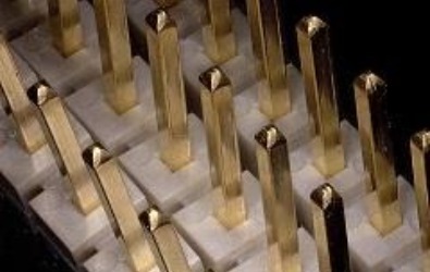
- Detection of part IC package defects, such as appearance integrity, the black gum cracks, pin deformation or discoloration.
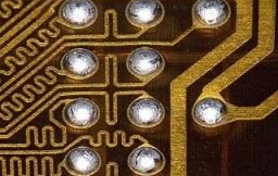
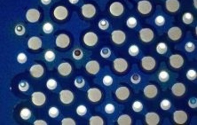
- Detection of potential PCB defects, such as nodules, weave exposure, glass fiber exposure, solder mask, text.。
- Detection of potential detects in electronic products, such as poor soldering.
- Detection of potential detects in electronic products, such as poor soldering.
- Appearance check and analysis of active and passive components.
- Analysis and measurement of all materials
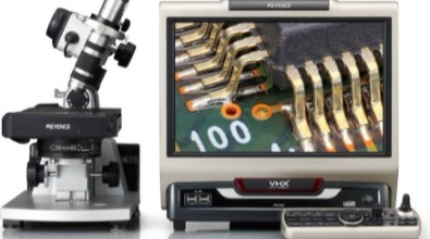
KEYENCE VHX-2000 Specification & Features
- Magnification:20X~1000X
- Tilt angle:0°~60°
- Rotation:180°
- Highly Composite Images
<Under high magnification observation, a fully focused image can also be obtained.>
- Fill Light Function(LED light source)
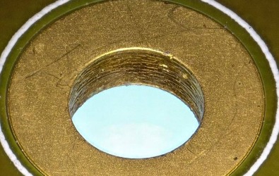
<The Fill Light Function with XY table moving system could give the full-angle observation. For via hole of PCB, the Fill Light function can be irradiated from bottom and check whether the via hole is plugged or damaged.>
- High Definition Dimensional Measurement
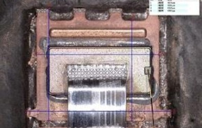
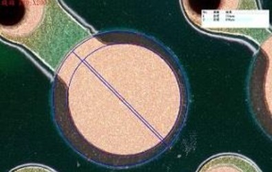
<Completely dimensional measurement includes length, angle, area and so on, and satisfies various request from clients.>
- High Speed Automatic Images Composite
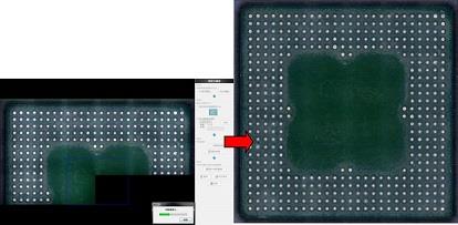
<Record and assemble images automatically to obtain wide-angle images through the XY table moving system>
To make all your PROBLEMS SOLVED, we provide professional consultant and service.
For more information or service, please feel free to email to 📧 sos@dekra-ist.com


